Edit Content

Our expertly engineered manufacturing services lay the foundation for smarter devices and seamless integration. Trust Kenoxis Technologies to deliver efficiency, reliability, and scalability every step of the way. Our team comprises experienced engineers, product designers, quality inspectors, and R&D specialists, all working in unison to bring innovative ideas to life.

Get in Touch

Contact Us

Email address

support@kenoxistechnologies.com

Phone Number

+1 855-673-5515

Office Address

1639 Western Park CT,
Dallas, Texas 75211, USA

Compact but Powerful: Designing Sleek All-in-One PC PCBs

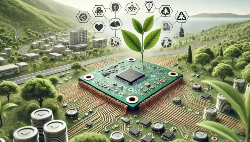
Introduction to All-in-One PC PCB Innovation The all-in-one (AIO) PC market has grown rapidly, fueled by demand for sleek, powerful, and space-saving devices. At the heart of these machines lies the printed circuit board (PCB), which integrates critical components like processors, memory, storage, and connectivity modules. Unlike traditional desktops, AIO PCs must balance compactness with high performance, making PCB design a core factor in delivering next-gen computing experiences. Modern PCB engineering isn’t just about connecting circuits—it’s about optimizing energy efficiency, ensuring thermal stability, and maintaining signal integrity in a constrained form factor. This article explores the strategies, materials, and innovations shaping sleek PCB designs for all-in-one PCs. Why Sleek PCB Design Matters in Compact Systems The demand for sleek, space-efficient, and powerful computing solutions has made all-in-one (AIO) PCs one of the most attractive categories in the tech industry. Unlike traditional desktops, which have the luxury of large chassis and multiple dedicated PCBs, AIO systems must condense every essential function into a compact board design. Space Optimization in PCB Layouts In AIO PCs, every millimeter matters. Engineers face the constant challenge of balancing functionality with available space. This involves: By leveraging multilayer PCB technologies, designers can embed power distribution planes, high-speed signal paths, and ground layers within a compact space. Enhancing User Experience with Slim Profiles End users demand thin and lightweight designs without compromising performance. Sleek PCB layouts directly influence how slim an AIO PC can be manufactured. A thinner system not only looks more modern but also: Ultimately, sleek PCB engineering isn’t just a technical necessity—it’s a core driver of market appeal. Core Principles of All-in-One PC PCB Engineering The foundation of a successful AIO PCB lies in the engineering principles that define reliability and performance. Designers must carefully balance power, signal integrity, and thermal performance to ensure smooth operation. Power Distribution and Energy Efficiency Efficient power management is critical. With multiple high-demand components running simultaneously, PCBs must: This ensures components such as CPUs and GPUs receive consistent power delivery without voltage fluctuations. Signal Integrity and High-Speed Data Flow Modern AIO PCs rely heavily on high-speed buses like PCIe, DDR memory, and USB-C. To maintain signal integrity, PCBs employ: Thermal Management and Heat Dissipation Heat buildup is one of the biggest challenges in compact PCBs. Without proper thermal management, performance suffers. Solutions include: By embedding thermal solutions directly within PCB design, manufacturers can minimize reliance on bulky external cooling systems. Advanced Materials Used in Modern PCBs Material science plays a critical role in enabling sleek PCB designs. Traditional FR4 substrates are no longer sufficient for high-speed, high-density AIO PCs. Multilayer PCB Technologies Modern AIO boards often feature 10–20 layers, allowing designers to separate power, signal, and ground planes while maintaining compactness. These multilayer boards support: Flexible and Rigid-Flex PCBs To achieve ultra-thin designs, engineers increasingly use rigid-flex PCBs, combining traditional rigid sections with flexible connectors. Benefits include: Eco-Friendly and Lead-Free Materials With rising environmental concerns, manufacturers are adopting halogen-free laminates, lead-free soldering, and recyclable substrates. Beyond compliance with regulations like RoHS and WEEE, this shift also improves brand reputation among eco-conscious consumers. Design Challenges in All-in-One PC PCB Development Creating PCBs for all-in-one PCs is a balancing act between performance, reliability, and compactness. While innovation has made sleeker designs possible, engineers face multiple technical obstacles that require smart solutions. Balancing Compactness with Performance The most pressing challenge is fitting desktop-class performance into a thin enclosure. Unlike desktops, AIO PCs don’t have room for: This means PCB engineers must: This balance ensures that users enjoy powerful performance while still benefiting from a slim form factor. Minimizing Electromagnetic Interference (EMI) With so many high-speed components placed close together, EMI becomes a significant problem. Poorly managed EMI can cause: To counter this, engineers implement: Durability and Long-Term Reliability All-in-one PCs are expected to last for years under heavy use. Reliability challenges include: To enhance durability, designers use high-Tg laminates (glass transition temperature materials), advanced underfill techniques for solder reinforcement, and thermal cycling tests during quality assurance. Integration of Key Components on PCB Unlike desktops, which distribute tasks across multiple boards, AIO PCs integrate almost everything on a single or minimal set of PCBs. This requires precision engineering for optimal placement. CPU and GPU Placement Strategies The CPU and GPU are the heart of performance. Engineers must ensure: Memory and Storage Integration Memory and storage require high-speed, stable connections. Integration strategies include: Connectivity Modules: WiFi, Bluetooth, and Ethernet Connectivity is critical for modern users. Engineers integrate modules directly onto PCBs using: By handling connectivity at the PCB level, manufacturers reduce the need for bulky external cards or dongles. Manufacturing Innovations for All-in-One PC PCBs Manufacturing sleek PCBs for AIO systems requires state-of-the-art production methods that go beyond traditional assembly lines. Automation in PCB Assembly Modern factories use robotic pick-and-place machines capable of positioning thousands of components per hour with microscopic precision. Benefits include: Quality Control and Testing Methods Since AIO PCBs handle multiple critical functions, testing is essential. Methods include: These innovations ensure that each PCB delivers long-term stability and performance before leaving the factory. Role of AI and Simulation Tools in PCB Design In recent years, artificial intelligence (AI) and simulation technologies have revolutionized PCB design for all-in-one PCs. As systems become more compact, manual trial-and-error methods are no longer sufficient. AI-powered platforms now assist engineers in: Simulation tools such as ANSYS, Cadence, and Altium Designer allow engineers to model entire PCB environments virtually. This not only reduces costs but also accelerates time-to-market by minimizing prototype iterations. By combining AI with simulation, PCB designers create smarter, more reliable boards that meet the demands of slim yet powerful AIO PCs. Cost-Effective Approaches Without Sacrificing Quality Designing sleek PCBs for AIO PCs can quickly become expensive due to the complexity of multilayer boards, premium laminates, and advanced manufacturing methods. However, cost can be controlled with the right strategies. Strategies for Cost Reduction Balancing Quality and Affordability While cost-saving is important, compromising on material quality or testing can lead to reliability issues. AIO

Next-Gen Camera PCBs: Design Trends Powering Smarter CCTV Solutions in 2025

Introduction: The Rise of Smart Surveillance Security is no longer just about cameras watching silently—it’s about intelligent systems that analyze, predict, and act in real time. The CCTV industry is witnessing a major transformation, fueled by Next-Gen Camera PCBs. These aren’t just circuit boards; they’re the brains and backbone of modern surveillance technology, ensuring sharper imaging, smoother data processing, and smarter connectivity. In 2025, surveillance solutions are increasingly expected to provide AI-driven analytics, energy efficiency, remote monitoring, and IoT compatibility. And none of this is possible without the advancements in PCB design. With smaller form factors, advanced heat management, and integration with wireless technologies, camera PCBs are redefining the capabilities of CCTV systems. What Are Camera PCBs and Why Do They Matter? Defining the Core Role of Camera PCBs A Camera PCB (Printed Circuit Board) is the structural and electronic foundation of a CCTV camera. It interconnects all critical components—sensors, processors, memory, and communication modules—allowing the camera to function effectively. Without the PCB, a surveillance camera wouldn’t capture or process images, store video feeds, or transmit data. Simply put, the PCB is the nervous system of any camera, dictating how well it performs in both standard and high-demand environments. How Camera PCBs Differ from Standard PCBs Unlike general PCBs found in everyday electronics, camera PCBs are purpose-built for imaging and surveillance applications. They require: These specialized demands make camera PCBs unique, more resilient, and performance-oriented compared to standard circuit boards. The Evolution of CCTV Systems with PCB Innovations From Analog to Digital Surveillance CCTV technology has come a long way. Traditional analog systems offered limited clarity and bulky designs. With digital PCBs, cameras became smarter—offering HD and 4K imaging, remote monitoring, and compact structures. Key milestones include: The Role of AI and Machine Learning The real revolution came with AI-powered PCBs. Today’s camera boards embed AI chips and ML algorithms, enabling features like: AI-ready PCBs transform cameras from passive devices into proactive guardians of security. Key Design Trends in Next-Gen Camera PCBs The year 2025 brings cutting-edge PCB design trends that directly impact CCTV performance. Miniaturization and High-Density Interconnect (HDI) Flexible and Rigid-Flex PCB Structures Energy-Efficient PCB Designs Heat Dissipation and Thermal Management Integration with Wireless Technologies (WiFi, 5G, Bluetooth) These trends make camera PCBs the driving force behind smarter and more adaptive CCTV solutions.

Eco-Conscious PCBs: Recyclable and Biodegradable Innovations

Introduction The world is facing a growing crisis of electronic waste (e-waste). With billions of electronic devices produced annually, discarded gadgets are piling up at alarming rates. At the heart of these devices lies the printed circuit board (PCB)—the foundation of modern electronics. Traditional PCBs, however, pose a significant environmental problem. This is where eco-conscious PCBs, designed to be recyclable or biodegradable, are reshaping the future of electronics. Understanding PCBs Printed circuit boards (PCBs) are the backbone of electronic devices, providing the necessary pathways for signals and power to flow. Typically made with fiberglass, epoxy resins, and copper, PCBs are sturdy and efficient but not environmentally friendly. Their complex mix of non-degradable materials makes recycling nearly impossible using conventional methods. The Problem with Conventional PCBs Conventional PCB production relies on hazardous chemicals like brominated flame retardants and heavy metals, which pose risks to both humans and the environment. When disposed of improperly, PCBs contribute heavily to toxic e-waste. Landfills become saturated with non-degradable materials, releasing harmful substances into soil and groundwater. Additionally, the energy-intensive production process of PCBs further increases the industry’s carbon footprint. What Are Eco-Conscious PCBs? Eco-conscious PCBs are designed with the environment in mind. Unlike traditional boards, these are created using recyclable or biodegradable materials. Their aim is to reduce waste, lower emissions, and support sustainable product lifecycles. Instead of persisting in landfills for centuries, eco-PCBs can either be dismantled for recycling or safely decompose without harming ecosystems. Recyclable PCBs Recyclable PCBs focus on making materials recoverable. Metals like copper, silver, and gold can be extracted, while substrates can be designed for reuse. These boards simplify disassembly and encourage circular economy models in electronics. By making PCBs recyclable, manufacturers can recover valuable resources, cut down raw material use, and minimize landfill waste. Biodegradable PCBs Biodegradable PCBs take sustainability a step further. Made with polylactic acid (PLA), hemp fibers, or other natural composites, these boards are capable of decomposing under natural conditions. They are particularly useful for low-power electronics such as sensors, medical implants, and disposable IoT devices. Instead of lingering for decades, they break down safely into organic matter. Materials Driving Innovation The development of eco-PCBs relies on advanced, sustainable materials: Manufacturing Processes Eco-friendly PCB manufacturing focuses on minimizing toxic waste and energy use. Low-toxicity etching solutions replace harmful acids, while laser-based and additive manufacturing reduce chemical reliance. Cleaner production not only protects workers but also lowers environmental impact. Performance vs. Sustainability A common concern is whether eco-PCBs perform as well as conventional boards. While biodegradable materials may not yet match fiberglass in durability, advances in composites and coatings are closing the gap. Recyclable PCBs, on the other hand, retain performance levels while simplifying material recovery. Applications of Eco-PCBs Eco-conscious PCBs are already finding applications in: Challenges in Adoption Despite the benefits, eco-PCBs face hurdles. Their production costs remain higher, limiting adoption in cost-sensitive industries. Some manufacturers are hesitant to switch due to performance concerns and supply chain adjustments. Scaling up eco-PCB production also requires infrastructure investment. The Role of Regulations Governments are stepping in with policies to tackle e-waste. Initiatives like the EU’s Waste Electrical and Electronic Equipment (WEEE) directive and India’s E-Waste Management Rules encourage manufacturers to adopt greener designs. Such regulations are accelerating the shift toward eco-conscious PCBs. Future Trends in PCB Sustainability The future looks promising for eco-PCBs. Innovations in AI-driven design, nanomaterials, and bio-based polymers will further enhance performance and sustainability. The electronics industry is steadily moving toward a circular economy, where components are reused and recycled endlessly. How Businesses Can Transition Businesses aiming for sustainability can adopt eco-PCBs by: Conclusion Eco-conscious PCBs are not just a trend—they are the future of electronics. By embracing recyclable and biodegradable innovations, the electronics industry can drastically cut down on e-waste, lower environmental harm, and move toward a truly sustainable future. Transitioning may come with challenges, but the long-term benefits for both businesses and the planet make it a necessity. FAQs 1. What makes a PCB biodegradable?Biodegradable PCBs are made using natural fibers and bio-polymers like PLA that decompose naturally without leaving toxic residue. 2. Are eco-PCBs as durable as traditional PCBs?Recyclable PCBs match conventional durability, while biodegradable ones are improving but may be more suited for short-term or disposable applications. 3. How can companies recycle PCBs?By designing boards with recyclable substrates and using processes that allow easy recovery of metals and components. 4. Are eco-PCBs cost-effective?Currently, they are more expensive than traditional PCBs, but costs are expected to decrease with wider adoption and better technology. 5. What industries benefit most from eco-PCBs?Consumer electronics, healthcare, renewable energy, and IoT industries stand to benefit significantly from eco-conscious PCBs.