Our expertly engineered manufacturing services lay the foundation for smarter devices and seamless integration. Trust Kenoxis Technologies to deliver efficiency, reliability, and scalability every step of the way. Our team comprises experienced engineers, product designers, quality inspectors, and R&D specialists, all working in unison to bring innovative ideas to life.
support@kenoxistechnologies.com
+1 855-673-5515
1639 Western Park CT,
Dallas, Texas 75211, USA
The steps involved in PCB design or PCB layout are the same whether you design it yourself or from us. The difference is in the experience. The general steps are as follows:
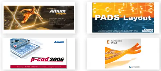
A PCB layout program is also required to draw the schematic and design the PCB layout. Common software includes Altium Designer, Pads, OrCAD, Eagle and P-CAD.
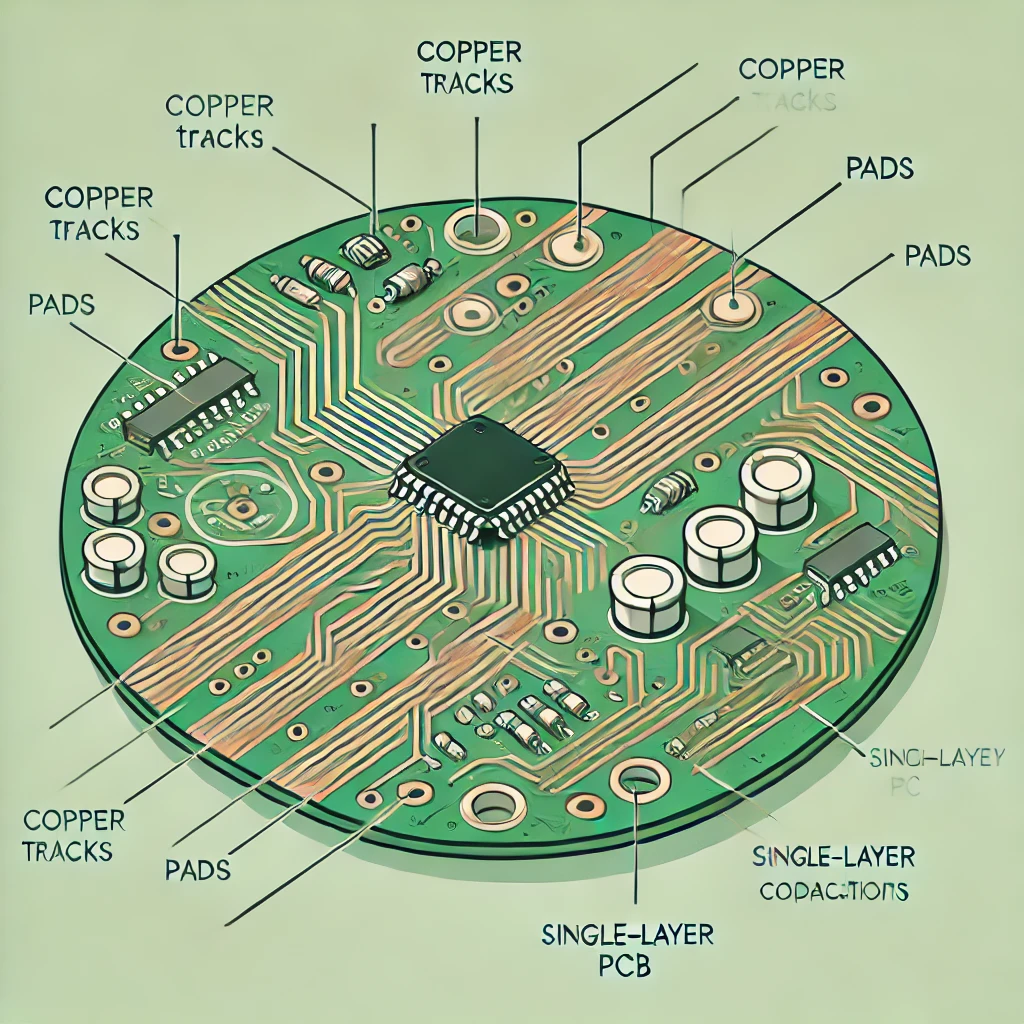
Kenoxis Technologies has a RandD team of circuit designers, development engineers, MCU and embedded system programmers to help you design a complex PCB to perfection. When you order from us, you don’t need to go through the above steps to get the final PCB layout, you just need to provide us with the circuit diagram, network list, component information and design requirements..
When designing a PCB, each layer of the PCB requires a Gerber file to be created for the PCB manufacturer to understand. Altium Designer Gerber files must be generated with three outputs, the steps are as follows: First Output
Print again
Third Output
Kenoxis Technologies offers one-stop RandD and PCBA production. Kenoxis Technologies PCB design services include:
Provide technical assistance including schematic analysis, PCB design, electrical principle design debugging and DFA design quality and reliability assurance.
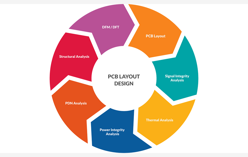
Kenoxis Technologies offers one-stop RandD and PCBA production. Kenoxis Technologies PCB design services include:
Provide technical assistance including schematic analysis, PCB design, electrical principle design debugging and DFA design quality and reliability assurance.
Get Best Quote by adding a few details of your
requirement